Types of printed circuit board
a ground plane or power plane, to achieve better signal integrity, higher signaling frequencies, and better power supply decoupling. In multilayer boards, layers of material are laminated together in an alternating sandwich: copper, substrate, copper, substrate, copper, etc.; each layer of copper is etched and any internal sleepers (which will not extend to PCB 2 Layer both
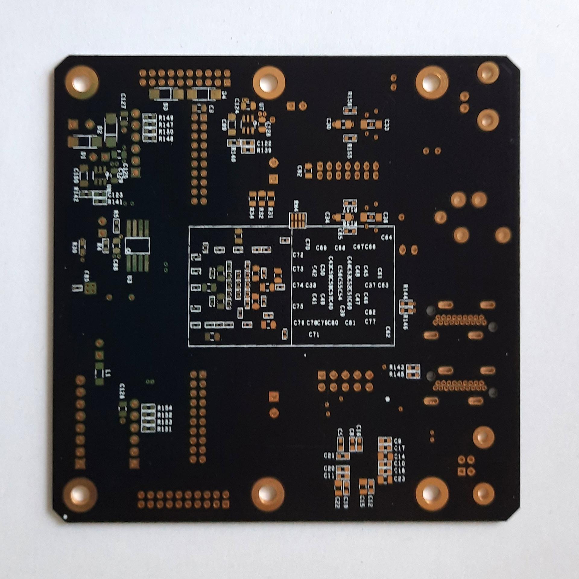
Printed circuit board construction
is designed with copper tracks (similar to wires on a flat surface) that provide electrical connections on that conductive layer. Another manufacturing process adds plated or metallized holes that allow interconnections between layers. PCBs mechanically support electronic components using pads for bonding the component terminals and electrically 2 Layer PCB connect them using
Properties of the printed circuit board
be laid out in a planar form, such as stripline or microstrip, with dimensions carefully controlled to ensure consistent impedance. In PCB Layer 2 RF and fast switching circuits, the inductance and capacitance of the printed circuit board conductors become significant, usually unwanted, circuit elements; rather, they can be used
